OPTOELECTRONIC AND SEMICONDUCTOR
WAFER AOI / DIE AOI / WIREBOND AOI / IC PACKAGE AOI
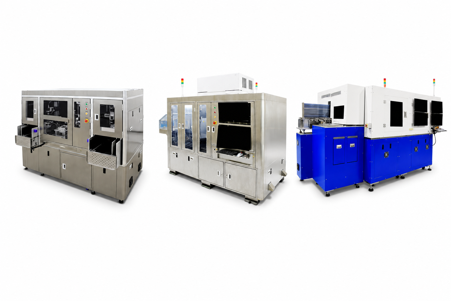
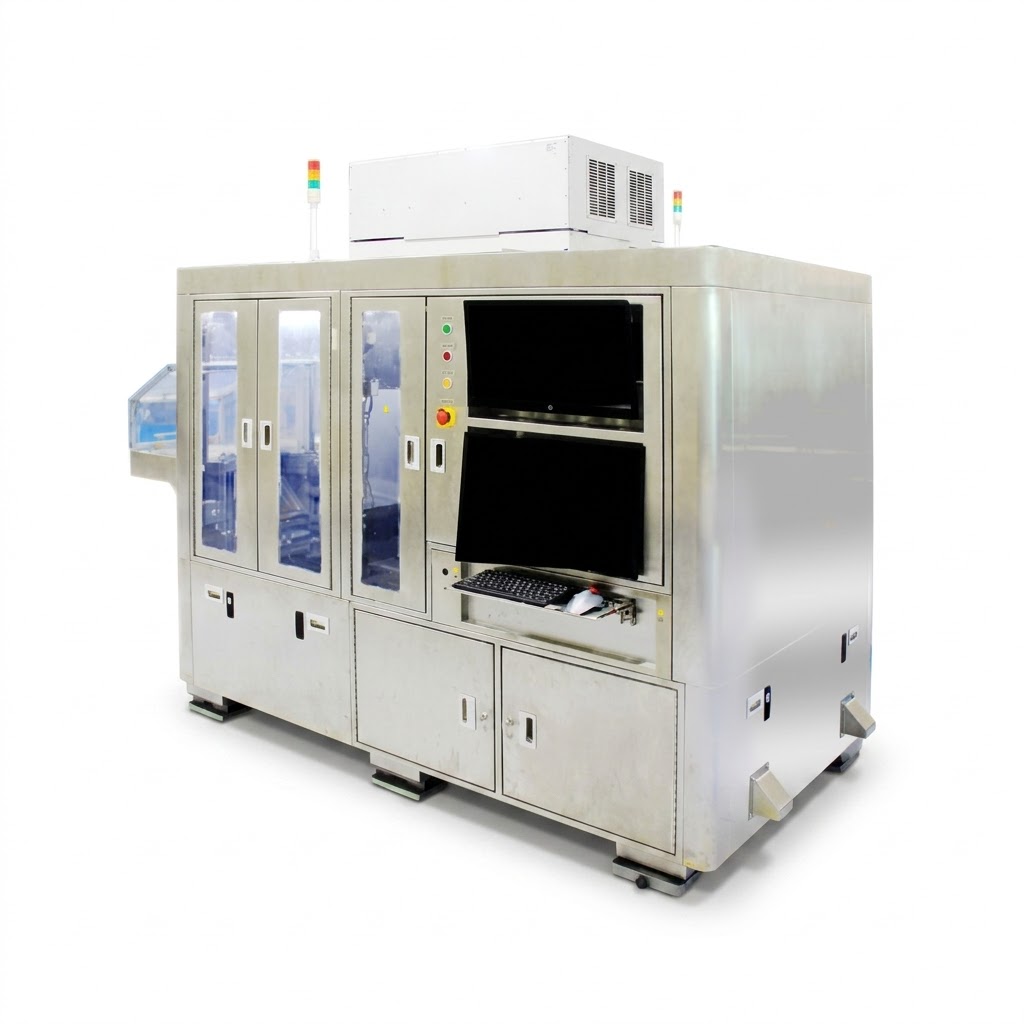
- ALPHA SERIES WFi-30 WAFER AOI
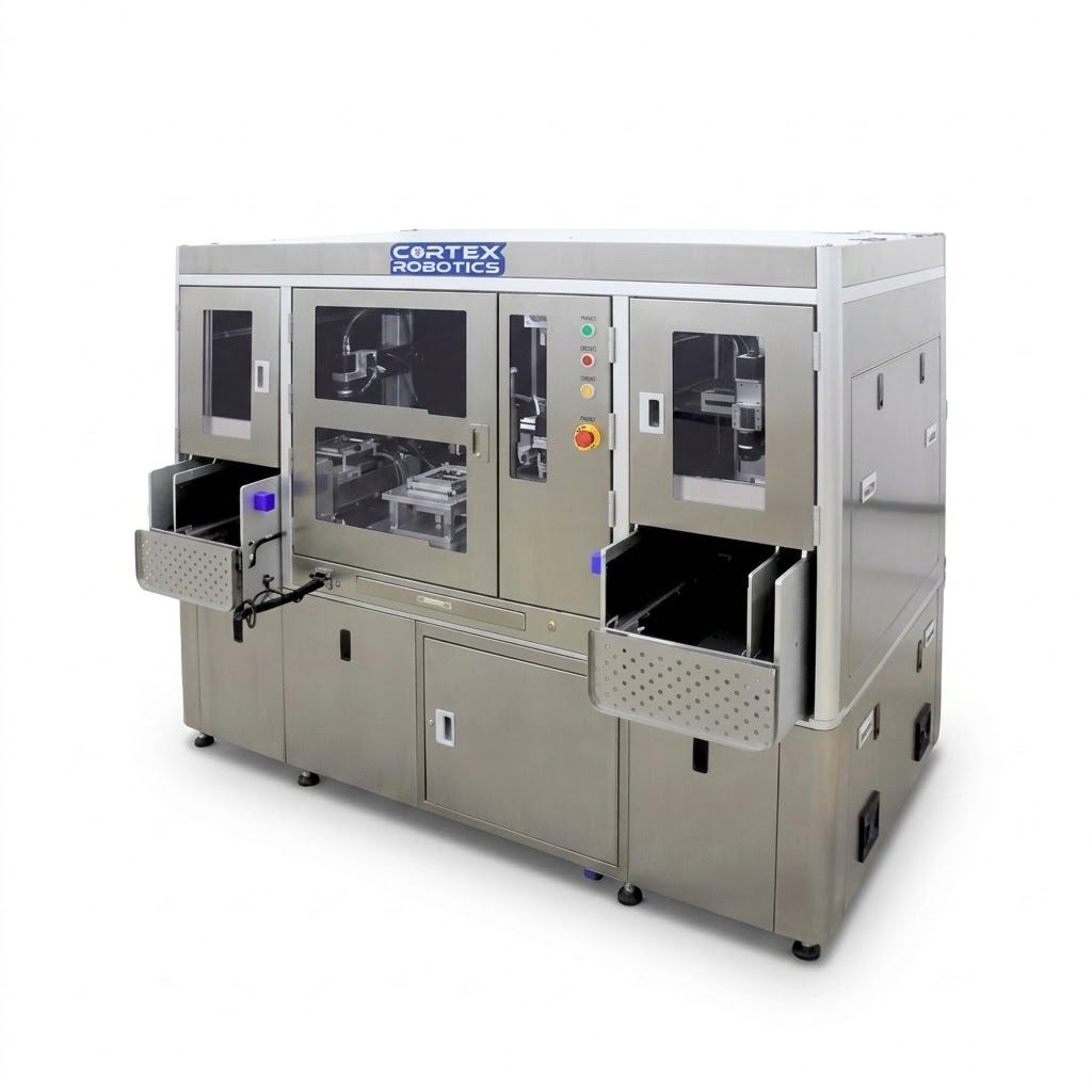
- VEGA SERIES DIE BOND AOI / WIRE BOND AOI
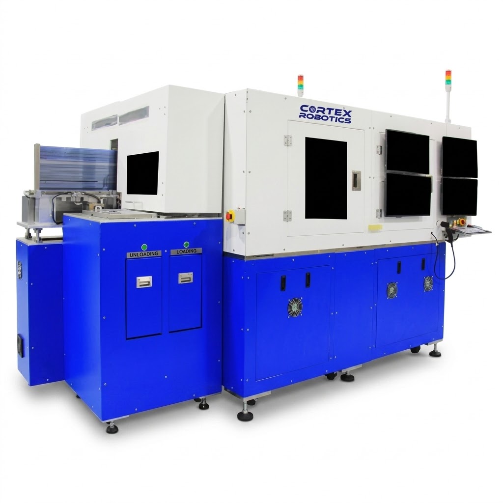
- METEOR SERIES IC PACKAGING AOI
ALPHA SERIES WFi-30 WAFER AOI
⭐ 1. High Throughput & Full Automation
Fully automated wafer inspection with dual loadports and robotic handling for maximum production efficiency.
⚡ 2. High Accuracy Defect Inspection
Provides precise detection of cracks, scratches, chipping, and wafer defects with advanced auto-focus technology.
🔍 3. Flexible & Advanced Inspection Technology
Supports 2D/3D and SWIR inspection technologies for comprehensive wafer analysis across multiple wafer sizes.
VEGA SERIES DIE BOND AOI / WIRE BOND AOI
⭐ 1. High Precision Bond Inspection
Provides accurate inspection for Die Bond and Wire Bond processes to ensure high product quality and reliability.
⚡ 2. Fast & Stable Automated Inspection
High-speed automated inspection system improves productivity and reduces manual inspection time.
🔍 3. Advanced Defect Detection Capability
Detects bonding defects such as wire deformation, missing bond, misalignment, and contamination with high accuracy.
METEOR SERIES IC PACKAGING AOI
⭐ 1. High Accuracy IC Package Inspection
Provides precise inspection for IC packaging processes to ensure product quality and reliability.
⚡ 2. High-Speed Automated Inspection
Supports fast and fully automated inspection for improved production efficiency and reduced cycle time.
🔍 3. Comprehensive Defect Detection
Detects various defects such as lead damage, marking defects, package cracks, contamination, and misalignment with high accuracy.
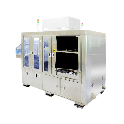
ALPHA SERIES WFi-30
WAFER AOI
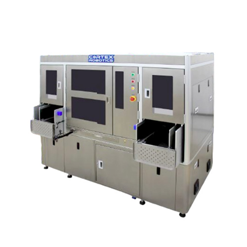
VEGA SERIES
DIE BOND AOI / WIRE BOND AOI
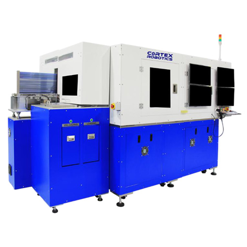
METEOR SERIES
IC PACKAGING AOI